| |
| META TOPICPARENT |
name="MoreSensors" |
Analogue to Digital and Digital to Analogue Conversion
The PCF8591 is a 4 channel analogue to digital (ADC) and 1 channel digital to analogue converter (DAC). ADC and DAC have 8 bit resolution. The PCB card already contains 3 devices that can be connected via jumpers to the ADC inputs: is a 4 channel analogue to digital (ADC) and 1 channel digital to analogue converter (DAC). ADC and DAC have 8 bit resolution. The PCB card already contains 3 devices that can be connected via jumpers to the ADC inputs:
|
|
<
< |
- a potentiometer on channel 0
- a photo resistor on channel 1
- a thermistor on channel 2
- channel 3 is free
|
>
> |
- a potentiometer on channel 3
- a photo resistor on channel 0
- a thermistor on channel 1
- channel 2 is free
|
| | The sensors are resistors whose resistivity changes with the parameter to be measured (temperature or light intensity) and, in conjunction with a 1 kΩ resistor they implement a voltage divider. This voltage is converted to a digital value by the ADC. |
|
>
> | There are 2 LEDs on the PCB: a red one showing that the board is powered and a green one connected to the DAC output. |
| | I used the forth channel to feed back the DAC output.
 |
 |
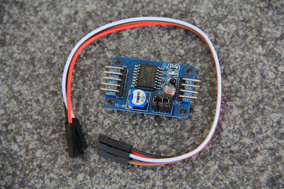
| pcf8591 front |
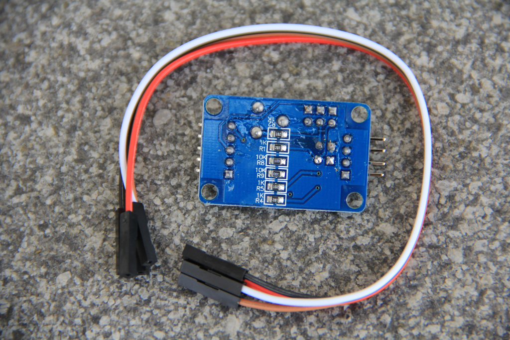
pcf8591 back |
You can distinguish the PCF8591 chip, the potentiometer and the photo resistor and thermistor. The pins on the left make the connections to external analogue signals and 1 pin provides the DAC output while the pins on the right implement the I2C interface with SCL, SDA, Vcc and Gnd. |
|
>
> | Here is the circuit diagram of the PCS:
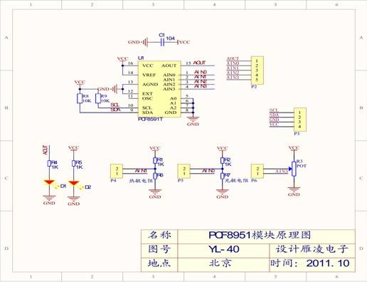 Unfortunately on the boards I purchased in China there is an error on the PCB: The thermistor is not correctly connected to ground. For this reason I only see the value 0xff. A little bridge between the ground pin of the photo resistor and the thermistor will do the trick.
 |
| | --  Uli Raich - 2017-02-01 Uli Raich - 2017-02-01
Comments |
| |
| META FILEATTACHMENT |
attachment="pcf8591back.png" attr="" comment="" date="1486214030" name="pcf8591back.png" path="pcf8591back.png" size="1248178" user="uli" version="1" |
| META FILEATTACHMENT |
attachment="pcf8591front.png" attr="" comment="" date="1486214039" name="pcf8591front.png" path="pcf8591front.png" size="1122628" user="uli" version="1" |
|
|
>
> |
| META FILEATTACHMENT |
attachment="yl-40.jpg" attr="" comment="" date="1486220007" name="yl-40.jpg" path="yl-40.jpg" size="38173" user="uli" version="1" |
|

 Unfortunately on the boards I purchased in China there is an error on the PCB: The thermistor is not correctly connected to ground. For this reason I only see the value 0xff. A little bridge between the ground pin of the photo resistor and the thermistor will do the trick.